GaSb single crystals can be used as substrate materials because of their lattice constants matching the lattice constants of various ternary and quaternary, III-V compound solid solutions with band gaps in the 0.8~4.3um wide spectral range. The limited mobility of GaSb lattice is greater than that of GaAs, making it a potential application prospect in the manufacture of microwave devices. Growth methods include LEC, VGF and VBG.
| Single Crystal | Doping | Conductivity Type | Carrier Concentration cm-3 | Mobility (cm2/V.s) | Dislocation Density (cm-2) | Standard Substrate | |
| GaSb | Intrinsic | P | (1-2)´1017 | 600-700 | £1´104 | Φ2″×0.5mm Φ3″×0.5mm | |
| GaSb | Zn | P | (5-100) ´1017 | 200-500 | £1´104 | Φ2″×0.5mm Φ3″×0.5mm | |
| GaSb | Te | N | (1-20)´1017 | 2000-3500 | £1´104 | Φ2″×0.5mm Φ3″×0.5mm | |
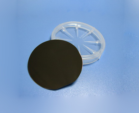
| Dimension(mm) | Dia50.8x0.5mm,10×10×0.5mm、10×5×0.5mm According to customer needs, substrates with special orientation and size can be customized. | ||||||
| Surface Roughness | Surface roughness(Ra):<=5A | ||||||
| Polishing | One side or two sides | ||||||
| Packaging | Clean bag (100), Super clean room (1000) | ||||||