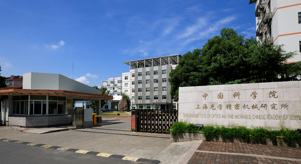
Shanghai Institute of Optics and Fine Mechanics, Chinese Academy of Sciences (abbreviated as: Shanghai Institute of Optics and Mechanics) was established in May 1964. It is the earliest and largest laser science and technology research institute in China. So far, it has formed a comprehensive research institute focusing on exploring the major foundations of modern optics and the frontiers of application foundations, developing large-scale laser engineering technologies, and exploring high-tech applications of lasers and optoelectronics. It is an important research, development and production base of laser and optical functional materials in my country, and it is also a training base for high-level materials science talents in my country.
The Micro-Nano Optoelectronics Functional Materials Laboratory of Shanghai Institute of Optics and Mechanics, Chinese Academy of Sciences was formally established in April 2018. It is a combination of the original Intensive Laser Materials Key Laboratory and the Optical Storage Laboratory, focusing on the development of nano-nonlinear optical effects, materials and applications, and phase Research on photoelectric functional films and devices, micro-nano structure photoelectric devices and systems, laser and optical ceramics, photoelectric functional crystals, big data storage, scientific and technological archaeology, etc.
The employees of the Optoelectronic Materials Division have many years of experience in crystal growth and processing, and possess a variety of crystal growth technologies and equipment such as the pulling method, the Kyrgyzstan method, the crucible descending method, the heat exchange method, and the optical floating zone method. Provide high-temperature superconducting film substrates, magnetic film and ferroelectric film substrates, semiconductor crystals, photoelectric crystals, laser crystals and other materials to scientific research institutes at home and abroad, and provide processing services such as orientation, cutting, grinding, and polishing of crystal materials. It can provide high quality (super smooth, super flat, super clean), multi-variety (more than 30 kinds, hundreds of specifications and sizes) of epitaxial film substrates and functional crystals, as well as high-purity, multi-specification sputtering targets (Single crystal target, ceramic target, metal target and alloy target).