With InAs single crystal substrate, InAsSb/In-AsPSb, InNAsSb and other heterojunction materials can be grown to produce infrared light-emitting devices with wavelengths of 2-14μm. InAs single crystal substrates can also be used to epitaxially grow AlGaSb superlattice structure materials. Mid-infrared quantum cascade laser. These infrared devices have good application prospects in gas monitoring, low-loss optical fiber communications and other fields. In addition, InAs single crystal has high electron mobility and is an ideal material for making Hall devices. As a single crystal substrate, InAs materials need to have low dislocation density, good lattice integrity, appropriate electrical parameters and high uniformity. The main growth method of InP single crystal materials is the traditional liquid-sealed Czochralski technology (LEC).
| Main performance parameters | |||||||
| Single Crystal | Dopant | Conduction Type | Carrier Concentration (cm-3) | Mobility (cm2/V.s) | Dislocation density (cm-2) | Standard substrate | |
| InAs | Undoped | N | 5´1016 | ³2´104 | <5´104 | Φ2″×0.5mm Φ3″×0.5mm | |
| InAs | Sn | N | (5-20) ´1017 | >2000 | <5´104 | Φ2″×0.5mm Φ3″×0.5mm | |
| InAs | Zn | P | (1-20) ´1017 | 100-300 | <5´104 | Φ2″×0.5mm Φ3″×0.5mm | |
| InAs | S | N | (1-10)´1017 | >2000 | <5´104 | Φ2″×0.5mm Φ3″×0.5mm | |
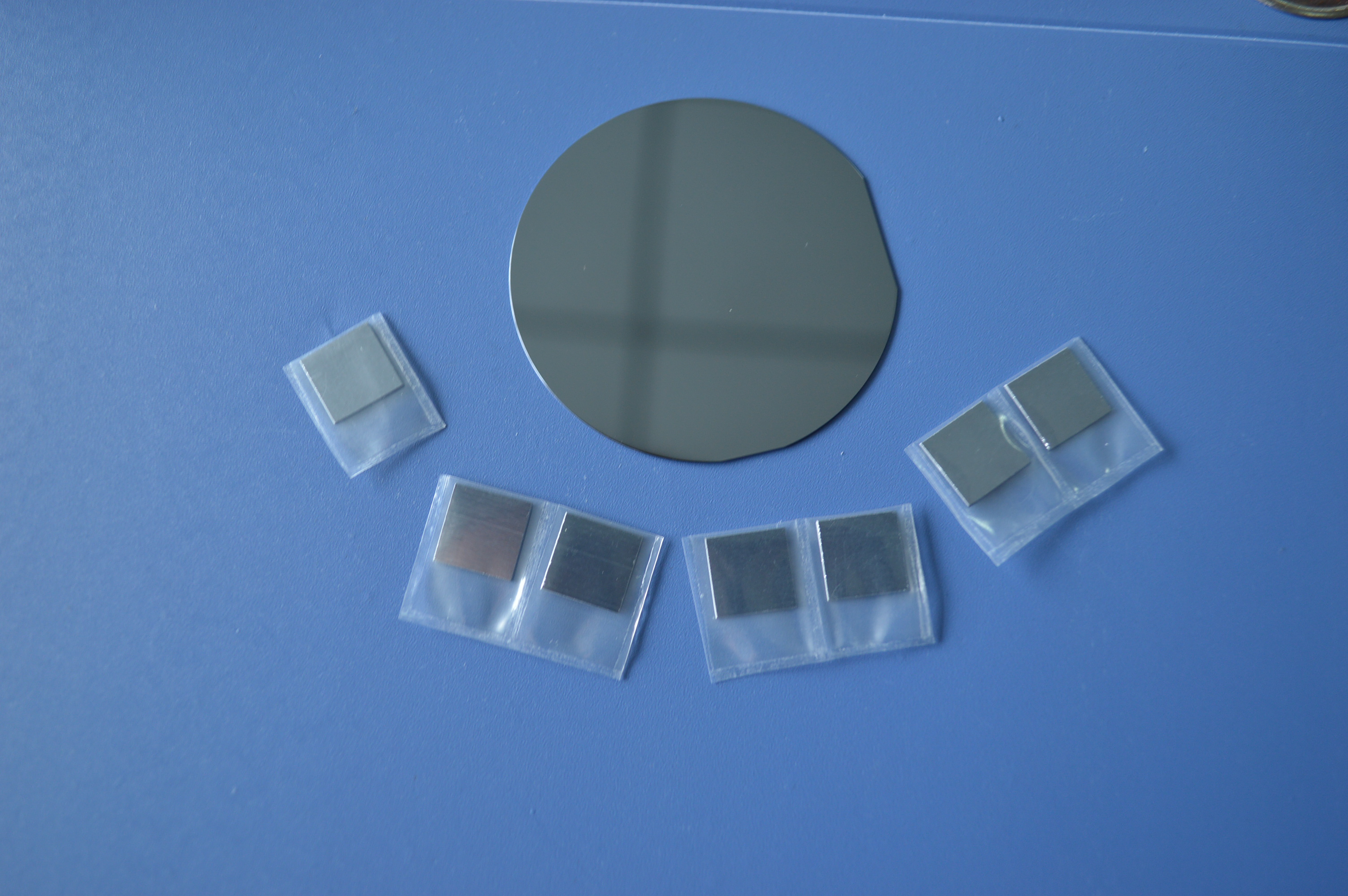
| Size(mm) | Dia50.8x0.5mm,10×10×0.5mm、10×5×0.5mm Can be customized according to customer needs, special direction and size of the substrate. | ||||||
| Surface roughness | Surface roughness(Ra):<=5A | ||||||
| Polishing | Single-sided or double-sided | ||||||
| Package | Class 100 clean bag, Class 1000 super clean room | ||||||